Designing a Simple System-on-a-Chip in Under 60 Minutes with the mu0 Microprocessor and Xilinx Tools
A demonstration of IP Core Technology in VHDL
Austin Rogers, Fall 2003
The mu0 is a microprocessor developed in VHDL. It is a very simple microprocessor, supporting only eight instructions and containing a single accumulator register. However, a simple example such as this provides a good introduction to the concept of design with Intellectual Property Cores. IP Cores are models developed by individuals and organizations, and licensed out for use in the design of digital systems. The use of IP Cores allows the modern digital designer to quickly design, simulate, and implement large, complex digital systems. For more information on the mu0 microprocessor, please consult these pages prepared by Dr. Aleksandar Milenkovic.
This tutorial will cover the design of a simple system-on-a-chip in VHDL, with an emphasis on the development and simulation of a testbench for the mu0 microprocessor. The mu0 and its associated RAM will be treated as black boxes, and we will develop a simple system around them.
1. Use Xilinx Project Navigator to set up the project folder
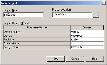
Start Xilinx Project Navigator. If it automatically opens a project, close it by clicking on File->Close Project. Create a new project by clicking on File->New Project. First enter "c:\" (without the quotation marks) in Project Location, and then enter "mu0demo" in Project Name. Make sure that all fields are set to the values in the figure on the left. Click on the OK button. Project Navigator will create the folder c:\mu0demo and put a new project file mu0demo.npl in that folder.
2. Unzip the mu0 source files into the project folder
Download this zip file and use your favourite compression/decompression program to unzip its contents into the folder you just created.
3. Add the mu0 source files into the project
In Project Navigator, click on Project->Add Sources. Navigate to the c:\mu0demo folder. Select all the .vhd files in that folder and click the Open button. For each of the .vhd files, you will be prompted to choose its source type. For each file, choose VHDL Module and press the OK button.

4. Create a VHDL file describing the system
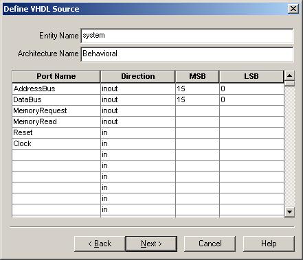
Click on Project->New Source. Select VHDL Module, and enter "system.vhd" (without quotation marks) as the File Name. Make sure the Location is specified as "c:\mu0demo". Press the Next button. You will now be asked to define the ports for entity system. Define them as in the figure below and press the Next button. Press the Finish button. Now the file system.vhd will be opened for editing.
5. Declare an instance of the mu0 and ram0 IP Cores
Add the following lines of code in the
architecture declaration, just BEFORE the begin statement:
|
|
component mu0 |
The preceding code
makes the mu0 and ram0 "black box" IP
Cores available for use in this design. Now initialize instances of the
mu0 and ram0 by adding the following
lines in the architecture section, just AFTER the begin statement:
|
|
A: mu0 port map(Clock, AddressBus, DataBus, Reset, MemoryRequest, MemoryRead); |
Save the file. Note that the tree view Sources in Project has been rearranged. mu0 and ram0 are now children of system.
6. Create the testbench file
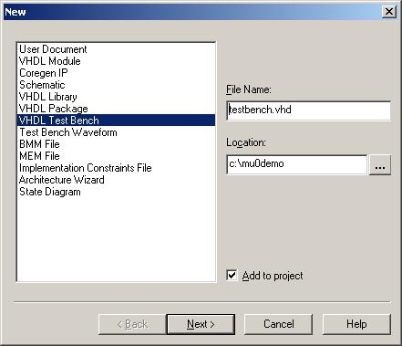
Click on Project->New Source. Select VHDL Test Bench, and enter the "testbench.vhd" (without quotation marks) as the File Name. Make sure that the Location specified is "c:\mu0demo" as in the figure below. Press the Next button. Then you will be prompted to select the source object with which to associate this testbench. Select system, then click the Next button. Then click the Finish button and inspect the testbench that has been created. Notice that it contains a declaration of the system defined in the previous step, and also the signals that will be used to interface with it. It also contains a process that does nothing but wait.
7. Provide a reset event
Add the following lines of code in the automatically
generated process, just before the wait statement.
|
|
Reset <= '1', '0' after 550 ns; |
8. Provide a clock
Add the following line of code in the architecture
just before the process (in between the line that reads *** Test Bench
- User Defined Section *** and the line that reads tb : PROCESS):
|
|
clock <= not clock after 50 ns; |
Now we must provide
an initial value for the clock. Modify the clock's signal declaration in
the architecture section, just before the begin statement. Change it to
the following:
|
|
SIGNAL clock : std_logic := '1'; |
Save your testbench file.
9. Set simulation time
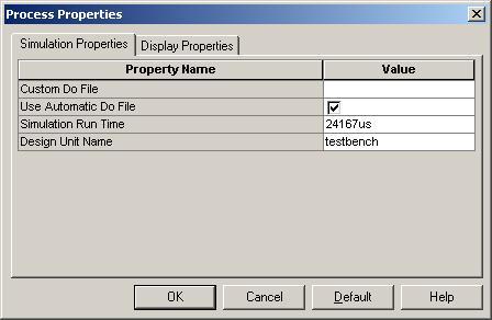
In the tree view Sources in Project, click on testbench.vhd. Then, in Processes for Current Source, right-click on Simulate Behavioral VHDL Model and select Properties. Make sure that Use Automatic Do File is selected, and set Simulation Run Time to 24167us as in the figure below. Press the OK button. Simulating for 24,167 microseconds will allow the whole program contained in ram0 to execute till completion.
10. Simulate the system in ModelSim
In Processes for Current Source, double-click on Simulate Behavioral VHDL Model. ModelSim will load and compile the VHDL files for this design. It should take several seconds for the simulation to complete. Once it stops, go to the "wave - default" window and maximize it. You should now zoom in or out depending on your preference. One good method is to click on View->Zoom->Zoom Full, and then do View->Zoom->Zoom In as many times as necessary. You may also change the radixes of the address and data busses back and forth between hexidecimal and binary if you wish. To do this, right-click on "/testbench/addressbus" in the left hand side of the "wave - default" window, and click on Radix->Hexadecimal or Radix->Binary. Repeat for "/testbench/databus" if desired. With patience, and an understanding of the mu0's instruction set, you will be able to trace the execution of the simple program.
11. Analyze the Program
Go back to the Xilinx Project Navigator. In the tree view Sources in Project, double click on ram0. This will open the ram0.vhd file for editing. Look at the definition of signal memory. This contains both the program and data memory to be used in the system. The simple program begins at the first address. It loads the contents of memory at address 16 (which initially contains 1) into mu0's accumulator. It adds to that the contents of memory at address 17 (which initially contains 2). It then subtracts from that the contents of memory at address 18 (which initially contains 1). This result is stored into memory at address 19. If the result is non-negative (that is, the sign bit is not set), it will repeat the sequence starting from the add statement. Notice that these math instructions are equivalent to incrementing the value of the accumulator by 1. It will continue incrementing until there is an overflow (when the addition of two positives produces a negative). It then subtracts the contents of memory at address 20 (which initially contains 8) and checks to see if the accumulator is zero. It will keep subtracting until the accumulator reaches zero, at which time execution will stop.